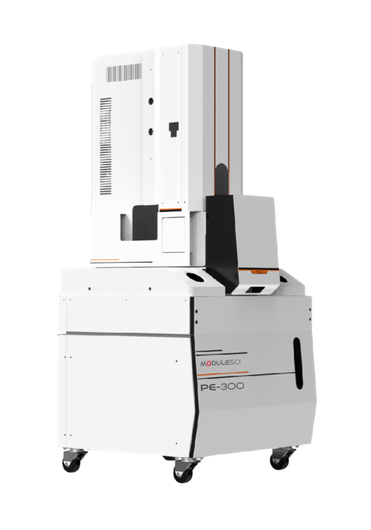
Key Features
- Advanced Schottky-type field emission electron source paired with a high-performance electron optical system for ultra-high imaging resolution
- Resolution of 0.9 nm at 15 kV and 1.3 nm at 1 kV, with high-quality imaging at both conventional and low accelerating voltages
- Low-voltage imaging observes non-conductive specimens directly, without conductive coating, preserving true surface morphology
- Integrates SE imaging, BSE imaging and EDS on a single platform for comprehensive morphology, microstructure and elemental characterization
- Rapid image acquisition with a large depth of field
- Large-travel sample stage and an In-lens Detector (ILD) alongside the standard secondary-electron detector
- Suited to research institutes, university laboratories and industrial quality control
Specifications
| Parameter | Specification |
|---|---|
| Emission source | Schottky-type thermal field emission electron source (ZrO/W) |
| Resolution | 0.9 nm @ 15kV, 1.3 nm @ 1kV |
| Magnification (photo) | 8× ~ 2,000,000× |
| Accelerating voltage | 0.02~30 kV |
| Detector | Secondary Electron Detector (ETD), In-lens Detector (ILD); optional Backscattered Electron Detector (BSED), EDS |
| Image format | TIFF, JPG, BMP, PNG |
| High vacuum mode | ≤2×10⁻⁵ Pa |
| Automatic stage | 5-axis |
| Stage moving range | X: 0~130 mm, Y: 0~130 mm, Z: 2~50 mm |
| Main unit dimensions | 1000(W) × 1500(D) × 1700(H) mm |
| Weight | 800 kg |
| Room requirements | 4m × 4m × 2m |
| Power supply | AC 110/220V (±10%), 50/60Hz, 4kW |
| Temperature & humidity | 21±4°C, ≤60%RH |
As a field-emission system, the PE-300 runs high vacuum only and uses low-voltage imaging — rather than a variable-pressure mode — to image non-conductive samples without coating. A tabletop model (PV-100P) and a compact floor-standing tungsten SEM (PE-100) are also available in the ModuleSci SEM range.
Application Examples
A sample of imaging results produced on the PE-300.
Porous Hollow SiO2 Spheres
5kV, SE imaging
Chitosan
20kV, SE imaging
RF Microsphere Aggregates
20kV, SE imaging
ZIF-8
20kV, SE imaging
Carbonized RF Spheres
20kV, SE imaging
Grain Particle Reference Standard
20kV, SE imaging
Intelligent Operating Software
ModuleSci’s self-developed SEM software captures an image in three guided steps: mount and set the sample, take a navigation image while the chamber evacuates, then navigate to the region of interest and capture the SEM image. Automatic brightness/contrast, focus and astigmatism adjustment run in the background, with live chamber monitoring throughout.
Photo-assist tools include dimension measurement, image mixing and gesture-based quick navigation, with optional image stitching for wide-field views.
Software at a Glance
- Workflow
- Mount sample → navigate & evacuate → locate ROI & capture
- Languages
- Korean, English, Chinese, French, German, Russian
- Photo-assist tools
- Dimension measurement, image mixing, gesture navigation, optional image stitching
Get A Free Instrument Consultation!
We can suggest products to our customers to make them the leaders in their respective industries.